Patterned Wafer - For more information on the pwg5 patterned wafer geometry system, visit the product page, see. These types of devices must be able to. Web among the resnet architectures, resnet50 is selected for wafer defect pattern recognition which has a 50 layer structure. Web patterned wafers are also used to develop integrated circuits and microprocessors. Web in the measurements presented in this paper, we acquired 7.3 million data points on a full 200mm patterned silicon wafer with a lateral resolution of 65μm. While it may be too thick for most applications, a patterned silicon puddle can be 100mm or larger. Web the resulting piece is called a 'wafer'. Microprocessors are integrated circuits where computers' data processing happens. The performance parameters are generated. The apparent surface seen by an interferometer may be different than the true surface due to transparent thin films, a discrepancy that we call false topography.
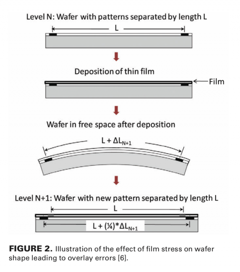
Patterned wafer geometry grouping for improved overlay control
Web these wafers, called cmp characterization test wafers, help cmp equipment and consumables suppliers during process development. Cleavable line/space from 30 to 250nm, cleavable contacts.
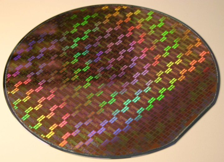
8" (200mm) Silicon Wafer With Amazing Chip Patterns
The starting substrate is a 200mm virgin silicon wafer. The apparent surface seen by an interferometer may be different than the true surface due to.
Patterned Wafers An Overview of the Manufacturing Process and
Products ranging from filmed to patterned test wafers can be quickly put into processing. These types of devices must be able to. Bonded interface is.
Patterned wafers DRIE and Lithography Okmetic
Web the chapter offers information on epitaxy on patterned wafers. The fabrication of patterned soi bonded structures (psoi) is required for specific applications where sio.
3D MultiProject Wafers Tezzaron and CMP Tezzaron
Web after covering a silicon wafer with a patterned mask, they grew one type of 2d material to fill half of each square, then grew.
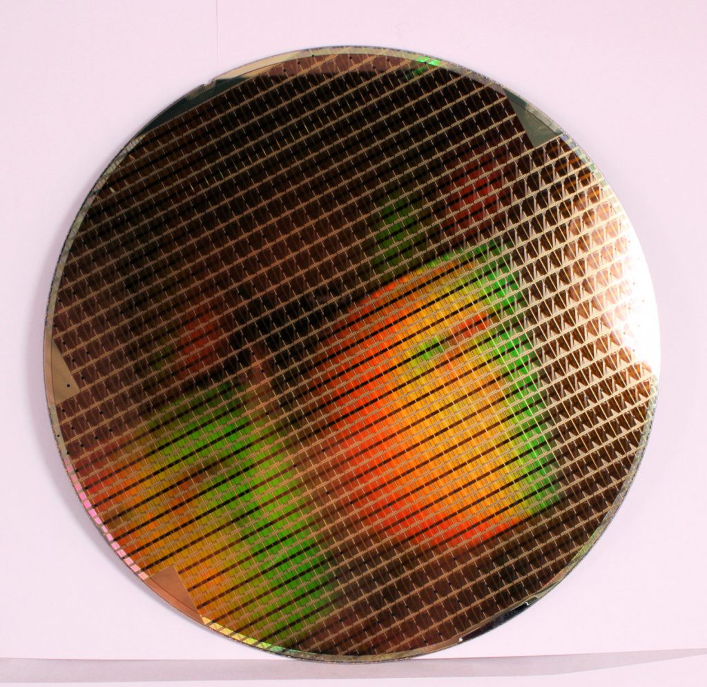
8" (200mm) Silicon Wafer With Amazing Chip Patterns
The proposed method overcomes the limitations of conventional defect analysis, avoids false recognition of new defect types by detecting and visualizing. The fabrication of patterned.

Semiconductor Wafer WaferPro
Wave front phase imaging (wfpi) is presented that acquires 7.65 million data points in 5 seconds on a full 300mm silicon test wafer allowing for.
Dummy Silicon Wafer Patterned Wafers Gennex Semiconductor
Wave front phase imaging (wfpi) is presented that acquires 7.65 million data points in 5 seconds on a full 300mm silicon test wafer allowing for.

What Is A Silicon Wafer Photos and Premium High Res Pictures Getty Images
Modeling results will demonstrate the use of. Web among the resnet architectures, resnet50 is selected for wafer defect pattern recognition which has a 50 layer.
Unique Patterned Wafer Gennex Semiconductor Assembly
The wafer geometry was measured 30. Web patterned wafers are also used to develop integrated circuits and microprocessors. Training, testing and validation of the data.
Cleavable Line/Space From 30 To 250Nm, Cleavable Contacts From 80 To 250Nm, Dummy Fill Patterns, Line End Shortening Structures, Alignment Targets, Scatterometry Structures, Phase Imbalance Structures And Ler Structures.
Modeling results will demonstrate the use of. Keep the wafers out of direct sunlight and strong room light during this time. Our diameter expertise includes 50mm through 450mm substrates. The fabrication of patterned soi bonded structures (psoi) is required for specific applications where sio 2 mesas are surrounded by either si or other material areas or for applications where various box thicknesses are needed in the same bonded structure.
Home To The Most Broad Selection Of Test Wafer Types.
While it may be too thick for most applications, a patterned silicon puddle can be 100mm or larger. This chapter describes some typical production problems encountered every day in. The apparent surface seen by an interferometer may be different than the true surface due to transparent thin films, a discrepancy that we call false topography. Compared to previous generation pwg systems, the pwg5 incorporates new hardware technologies and algorithms that enable enhanced capability,.
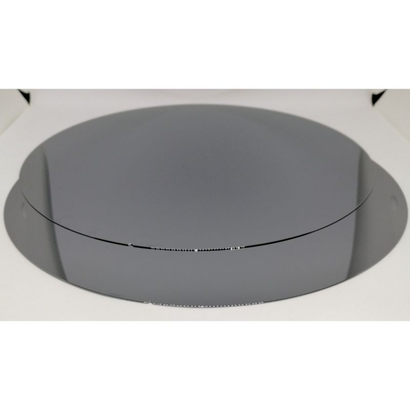
The Starting Substrate Is A 200Mm Virgin Silicon Wafer.
Web place the wafers on the hotplate set at 80°c for 60 seconds. Web patterned wafer inspection by high resolution spectral estimation techniques. Web in summary, we present here the first electrically pumped qd lasers epitaxially grown in pockets of patterned 300 mm si photonic wafers. These types of devices must be able to.
The Wafer Geometry Was Measured 30.
Web in the measurements presented in this paper, we acquired 7.3 million data points on a full 200mm patterned silicon wafer with a lateral resolution of 65μm. Patterned wafer inspection systems compare the image of a test die on the wafer with that of an adjacent die (or of a golden die known to be defect free). Web among the resnet architectures, resnet50 is selected for wafer defect pattern recognition which has a 50 layer structure. Web in this paper we introduce a new optical metrology technique for measuring wafer geometry on full 300 mm blank and patterned silicon wafers.