Pattern Wafers - Neapolitan cookies mix chocolate, vanilla , and strawberry for a visually appealing and flavorful treat. Web advantiv maintains an extensive inventory of silicon wafers. Web wafer defect inspection system detects physical defects (foreign substances called particles) and pattern defects on wafers and obtains the position coordinates (x, y) of the defects. I n this step, the pattern on the mask is transferred to the wafer by interaction of light with the photoresist. Web place the wafers on the hotplate set at 80°c for 60 seconds. Web i am reaching out because my research lab is interested to purchase some patterned silicon wafers. It is also used by ic manufacturers to ensure that incoming. Products ranging from filmed to patterned test wafers can be quickly put into processing. Web a planar or pattern film wafer is a more complicated substrate to make. Mit754 cu oxide patterned wafer.

The Evolution Of Patterned Wafers Past, Present, And Future Owlgen
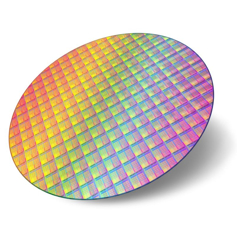
Web wafer map pattern classification. Manufactured at a 45nm idm in asia. A patterned silicon wafer is created using a process known as photolithography. Web.
Understanding Patterned Silicon Wafers Applications And Advantages
Desired areas of resist are exposed with uv light followed by development and etching. Mit754 cu oxide patterned wafer. The process involves developing patterns on.
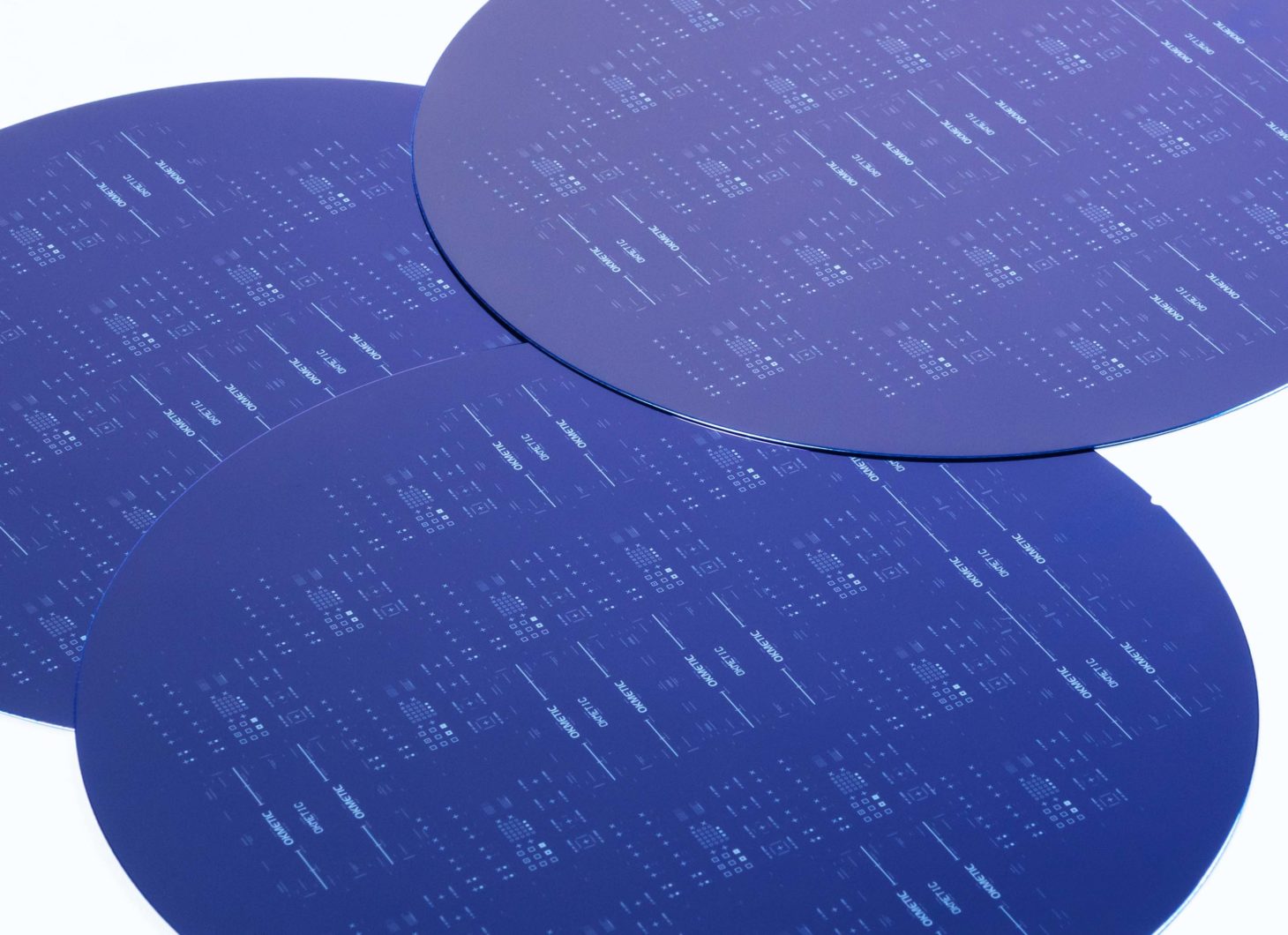
Patterned wafers DRIE and Lithography Okmetic
Web a planar or pattern film wafer is a more complicated substrate to make. Cleavable line/space from 30 to 250nm, cleavable contacts from 80 to.
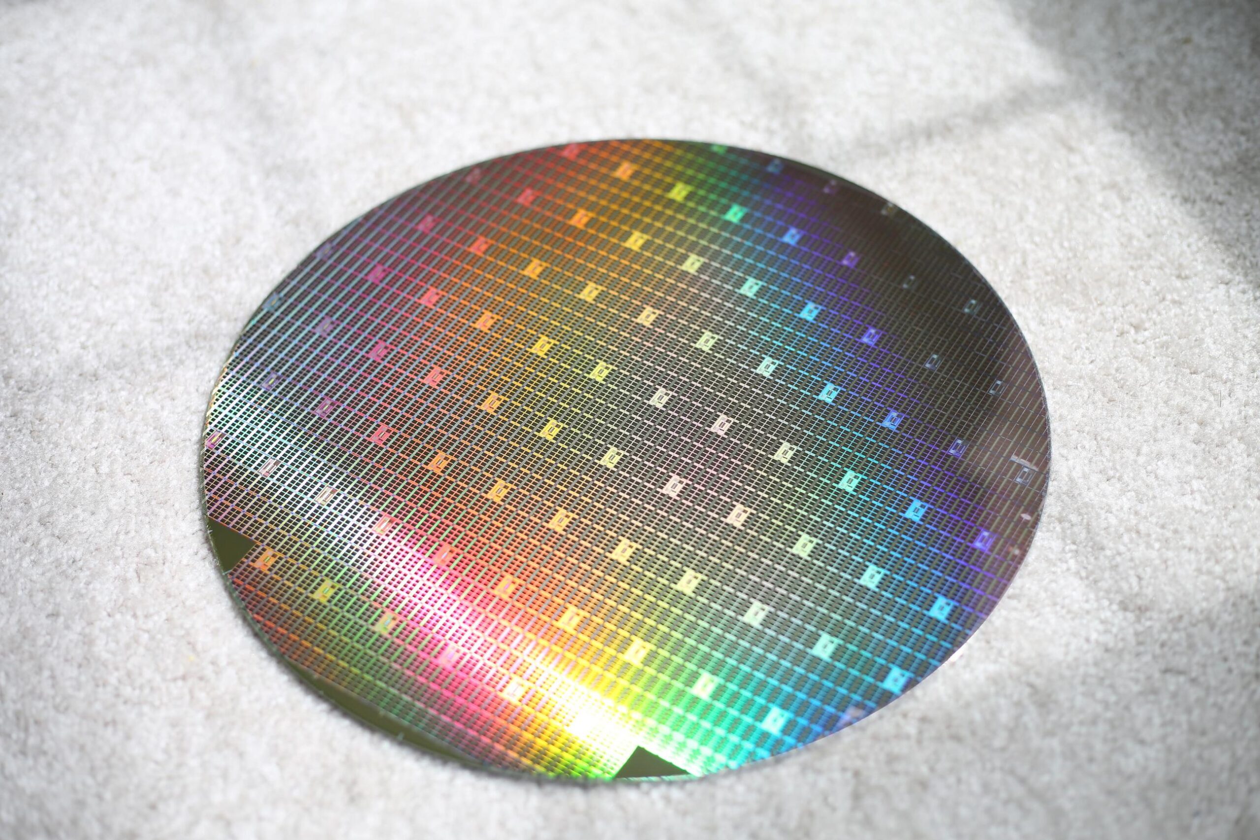
8" (200mm) Silicon Wafer With Amazing Chip Patterns
It's also easier to manage. Some of these advantages include better uniformity, greater reliability, and less variability. In addition, this paper draws a confusion matrix.
Patterned Wafers An Overview of the Manufacturing Process and
Mit754 cu oxide patterned wafer. Training, testing and validation of the data set is done. Wafer surface is then coated with photosensitive material. Some of.
How Patterned Wafers Are Made Exploring the Manufacturing Process
Web place the wafers on the hotplate set at 80°c for 60 seconds. Our diameter expertise includes 50mm through 450mm substrates. Web these wafers, called.
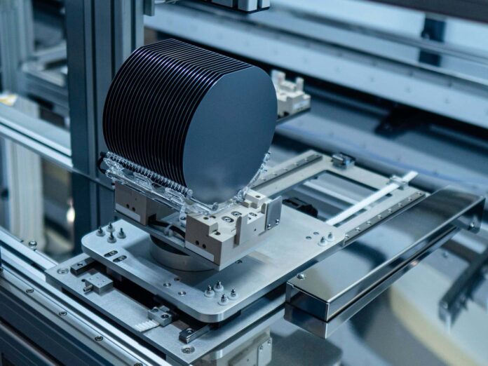
Unique Patterned Wafer Gennex Semiconductor Assembly
Defects can be divided into random defects and systematic defects. Web a planar or pattern film wafer is a more complicated substrate to make. It.

Wafer seamless pattern Royalty Free Vector Image
Web generally, wafer inspection is split into two categories—unpatterned and patterned. The capability is used for qualification and monitoring of process tools to capture blanket.

Semiconductor Wafer WaferPro
Defects can be divided into random defects and systematic defects. Patterned inspection detects defects on processed wafers. This reduced the possibility for variation in local.

8" (200mm) Silicon Wafer With Amazing Chip Patterns
Neapolitan cookies mix chocolate, vanilla , and strawberry for a visually appealing and flavorful treat. Web generally, wafer inspection is split into two categories—unpatterned and.
Proven Defect Performance, 4X Lower Defectivity Vs Industry Standard.
I n this step, the pattern on the mask is transferred to the wafer by interaction of light with the photoresist. As a result of this analysis, in manufacturing sti cmp process, we could use the removal rate of blanket wafer, which was changed by linear reduction as polishing time because of using the two data of the. The process involves developing patterns on a wafer's surface using light as we mentioned earlier. Patterned inspection detects defects on processed wafers.
Grid Is A Repeating Defect Pattern That Appears In Multiple Wafers, So Identifying Such Patterns Helps To.
It's also easier to manage. If the pattern is complex, it can be stacked on top of a planar or pattern film. The performance parameters are generated. Keep the wafers out of direct sunlight and strong room light during this time.
In Simple Terms, Unpatterned Wafer Inspection Looks For Defects On Unprocessed Or Bare Silicon Wafers.
Web i am reaching out because my research lab is interested to purchase some patterned silicon wafers. Wafer surface is then coated with photosensitive material. Neapolitan cookies mix chocolate, vanilla , and strawberry for a visually appealing and flavorful treat. Cleavable line/space from 30 to 250nm, cleavable contacts from 80 to 250nm, dummy fill patterns, line end shortening structures, alignment targets, scatterometry structures, phase imbalance structures and ler structures.
It Is Also Used By Ic Manufacturers To Ensure That Incoming.
Acerboni 9 wafer surface preparation 9 pattern integrity preservation in terms of geometrical issues 9 pattern integrity preservation in terms of doping 9 defect minimization, when introduced before and during the epi. Defects can be divided into random defects and systematic defects. A patterned silicon wafer is created using a process known as photolithography. Specially, recognizing grid, including line and intersection point types in wafer defect patterns is a challenging problem for process and test engineers.