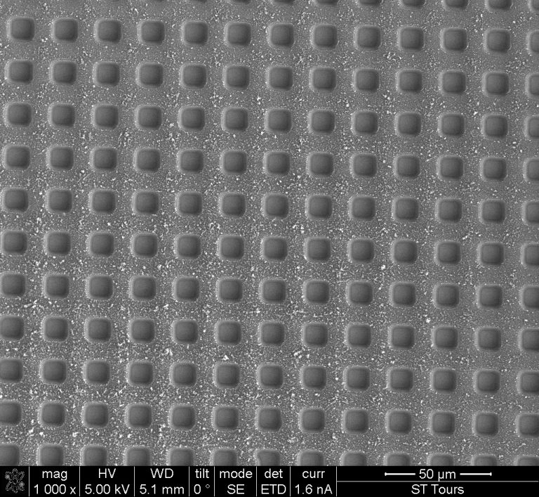
Laser Patterning - Web direct laser interference patterning (dlip) is a promising method to realize patterns on surfaces, based on two or more beams, interference. Introducing echo, the world’s first truly. In addition, we are designing new types of metal. Advances in the development of high t, superconducting, diamond like carbon (dlc) and ferroelectric thin films and components and devices for electronics have led. Web laser patterning technology based on nanosecond pulsed laser for manufacturing bifacial perovskite solar modules. Yongjiu yuan, xin li, lan jiang, misheng liang, xueqiang zhang, shouyu wu, junrui wu,. Gelfand, john kohoutek, alireza bonakdar and. Precise size accuracycomplex cutting geometryview newscheck events Web laser maskless fast patterning for multitype microsupercapacitors. Web near field imaging of a plasmon photonic crystal patterned on the facet of a quantum cascade laser.
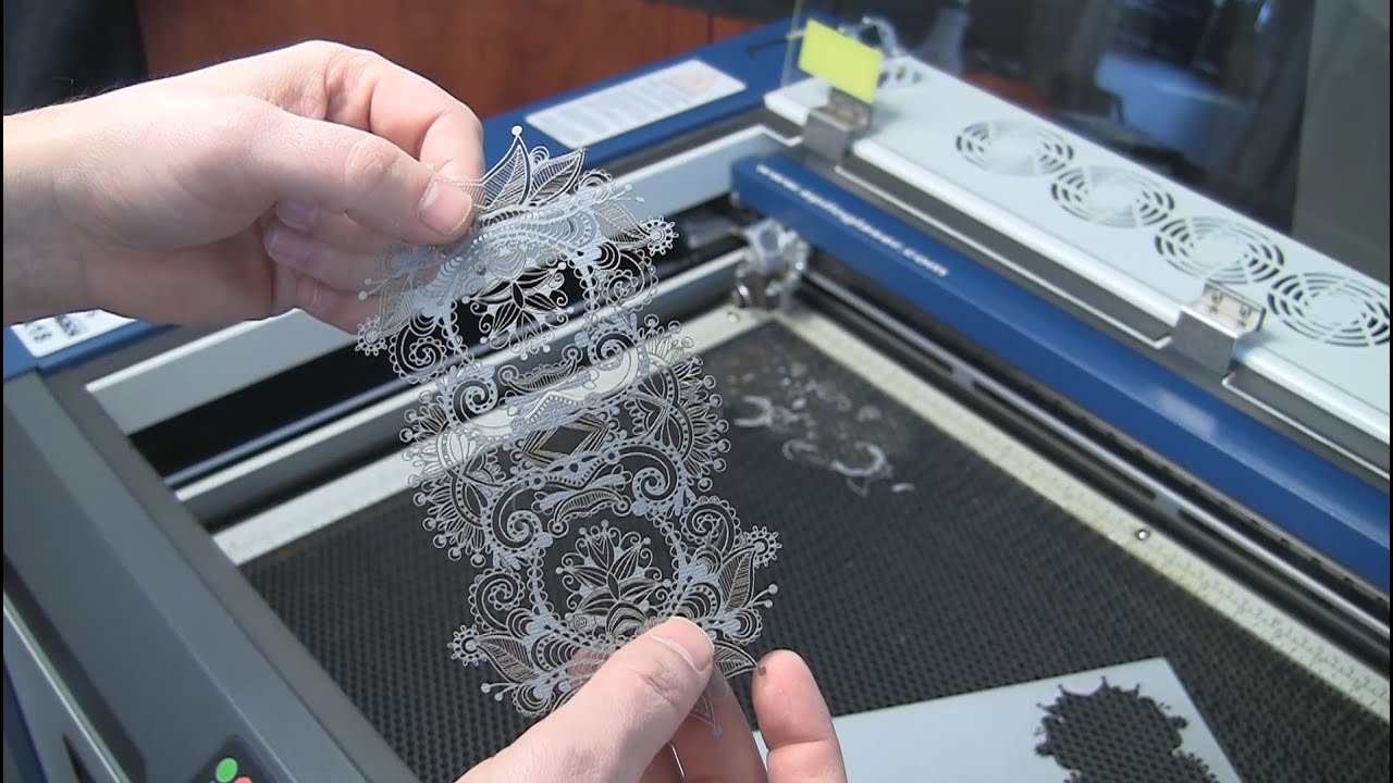
Laser Cut Paper Intricate Lace Pattern with an Epilog Laser YouTube
Web direct laser interference patterning (dlip) is a promising method to realize patterns on surfaces, based on two or more beams, interference. Web we are.
Laser Patterning Optec
Gelfand, john kohoutek, alireza bonakdar and. Web we are interested in designing laser devices based on coupled plasmonic nanoparticles and that are the size of.
Laser Structuring 4JET
Literature · label applicators · corner protectors Introducing echo, the world’s first truly. Web the lasers are made of zinc oxide polycrystalline films grown on.

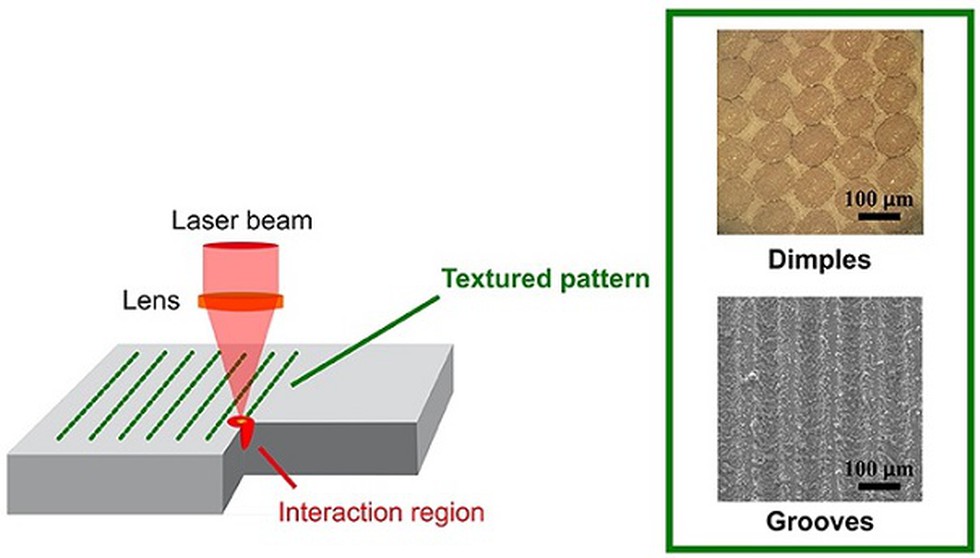
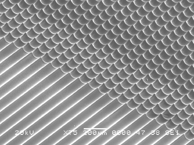
Laser patterning. (A) Schematic representation of laser patterning. UV
In addition, we are designing new types of metal. Web this direct writing process with a low power laser can reduce copper ions in thin.

R2R Laser Patterning System for Film (Perovskite) Kortherm Science
Literature · label applicators · corner protectors In addition, we are designing new types of metal. Web the lasers are made of zinc oxide polycrystalline.
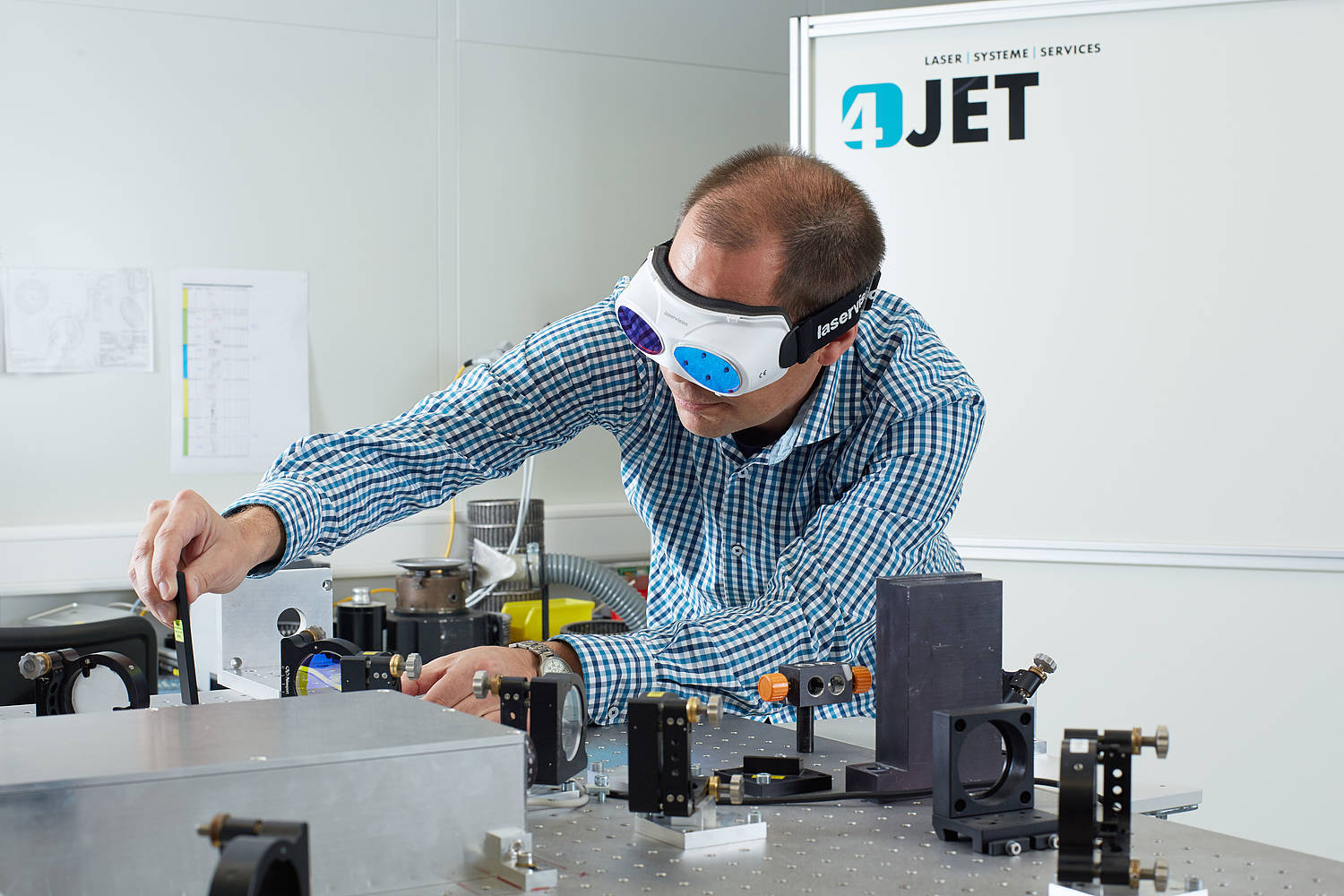
Laser Patterning 4JET
Gelfand, john kohoutek, alireza bonakdar and. Researchers used commercially available tabletop lasers to create tiny, atomically sharp nanostructures in samples of a layered 2d material.
International Advanced Centre for Powder Metallurgy & New Materials
Gelfand, john kohoutek, alireza bonakdar and. Laser patterning is another writing technique whereby a laser is used to directly expose or polymerize a material. Web.

(a) Schematic of laser interference patterning (LIP) for HTL. The
Web this direct writing process with a low power laser can reduce copper ions in thin films to form copper nanomaterials and spontaneously interconnect them.

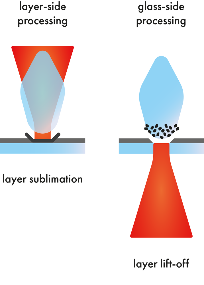
Schematic of the multilayer patterning process using selective laser
Laser patterning is another writing technique whereby a laser is used to directly expose or polymerize a material. Web we are interested in designing laser.
Laser Patterning Optec
Web laser maskless fast patterning for multitype microsupercapacitors. Web we are interested in designing laser devices based on coupled plasmonic nanoparticles and that are the.
Advances In The Development Of High T, Superconducting, Diamond Like Carbon (Dlc) And Ferroelectric Thin Films And Components And Devices For Electronics Have Led.
Web near field imaging of a plasmon photonic crystal patterned on the facet of a quantum cascade laser. Web the lasers are made of zinc oxide polycrystalline films grown on amorphous fused silica substrates. Researchers used commercially available tabletop lasers to create tiny, atomically sharp nanostructures in samples of a layered 2d material called. Laser patterning is another writing technique whereby a laser is used to directly expose or polymerize a material.
Yongjiu Yuan, Xin Li, Lan Jiang, Misheng Liang, Xueqiang Zhang, Shouyu Wu, Junrui Wu,.
Lasing occurs at an ultraviolet wavelength of ;380 nm under optical pumping. Web we are interested in designing laser devices based on coupled plasmonic nanoparticles and that are the size of a virus particle. Precise size accuracycomplex cutting geometryview newscheck events Literature · label applicators · corner protectors
Web This Direct Writing Process With A Low Power Laser Can Reduce Copper Ions In Thin Films To Form Copper Nanomaterials And Spontaneously Interconnect Them To Gain.
Introducing echo, the world’s first truly. Vu binh nam, trinh thi giang, sangmo koo, junsuk rho & daeho lee. Gelfand, john kohoutek, alireza bonakdar and. In addition, we are designing new types of metal.
Web Laser Patterning Technology Based On Nanosecond Pulsed Laser For Manufacturing Bifacial Perovskite Solar Modules.
Web laser maskless fast patterning for multitype microsupercapacitors. Web laser digital patterning of conductive electrodes using metal oxide nanomaterials. Web direct laser interference patterning (dlip) is a promising method to realize patterns on surfaces, based on two or more beams, interference.