Land Pattern - Lga + pin qty + c + pitch p + pin columns x pin rows _ body length x body width x height. Web generic requirements for surface mount design and land pattern standard. Web the landscapemetrics and motif packages for measuring landscape patterns and processes. The land pattern on a circuit board matches the arrangement of leads on a component. Land grid array, square lead. Not surprisingly, economic geographers use economic reasons to explain the location of economic activities. It includes the types of land uses that are present, such as residential, commercial, industrial, agricultural, and natural, as well as the spatial arrangement of these land uses. Here, the pitch p between pads is equal to the ideal pitch between leads on the component. Surface mount land patterns, also referred to as footprints or pads, define the sites at which components are to be soldered to a printed circuit board. Web the land pattern refers to the size of the pads and outline for a given part that should be designed onto a pcb.

topographic pattern design with shadows Download Free Vector Art
It is also important to note that land patterns should always match with the arrangements of lead. To come up with a land pattern, you.
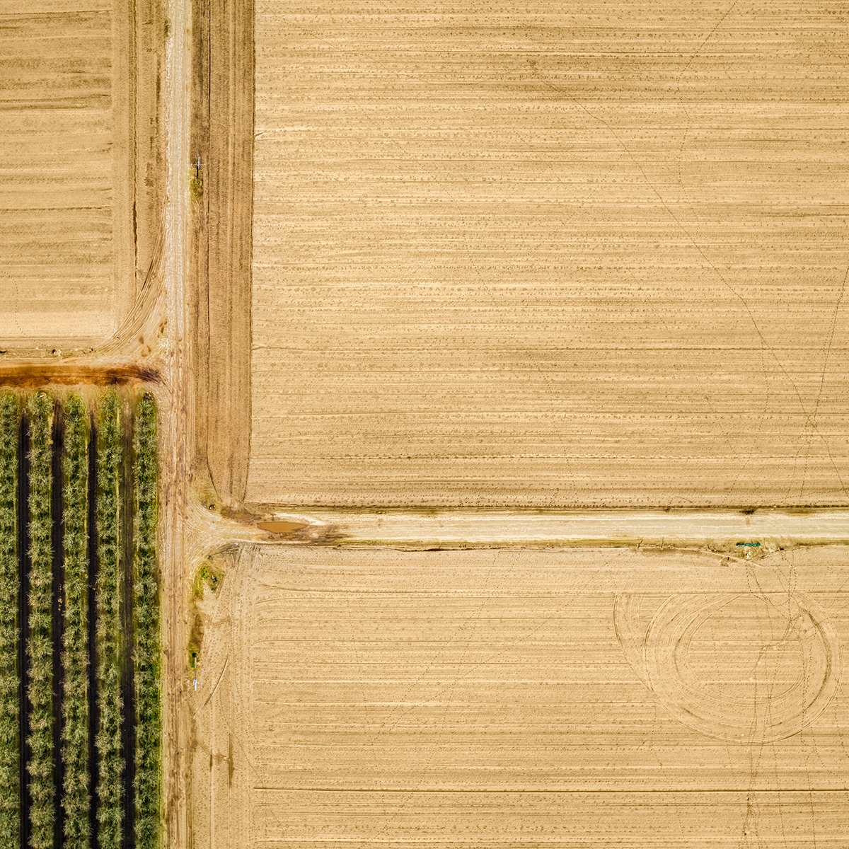
Project 17 Agricultural Aerial Land Patterns 1 on Behance
Land pads are always a little larger than part pads. Web what is the land pattern. Land patterns specify where copper will exist on fabrication.
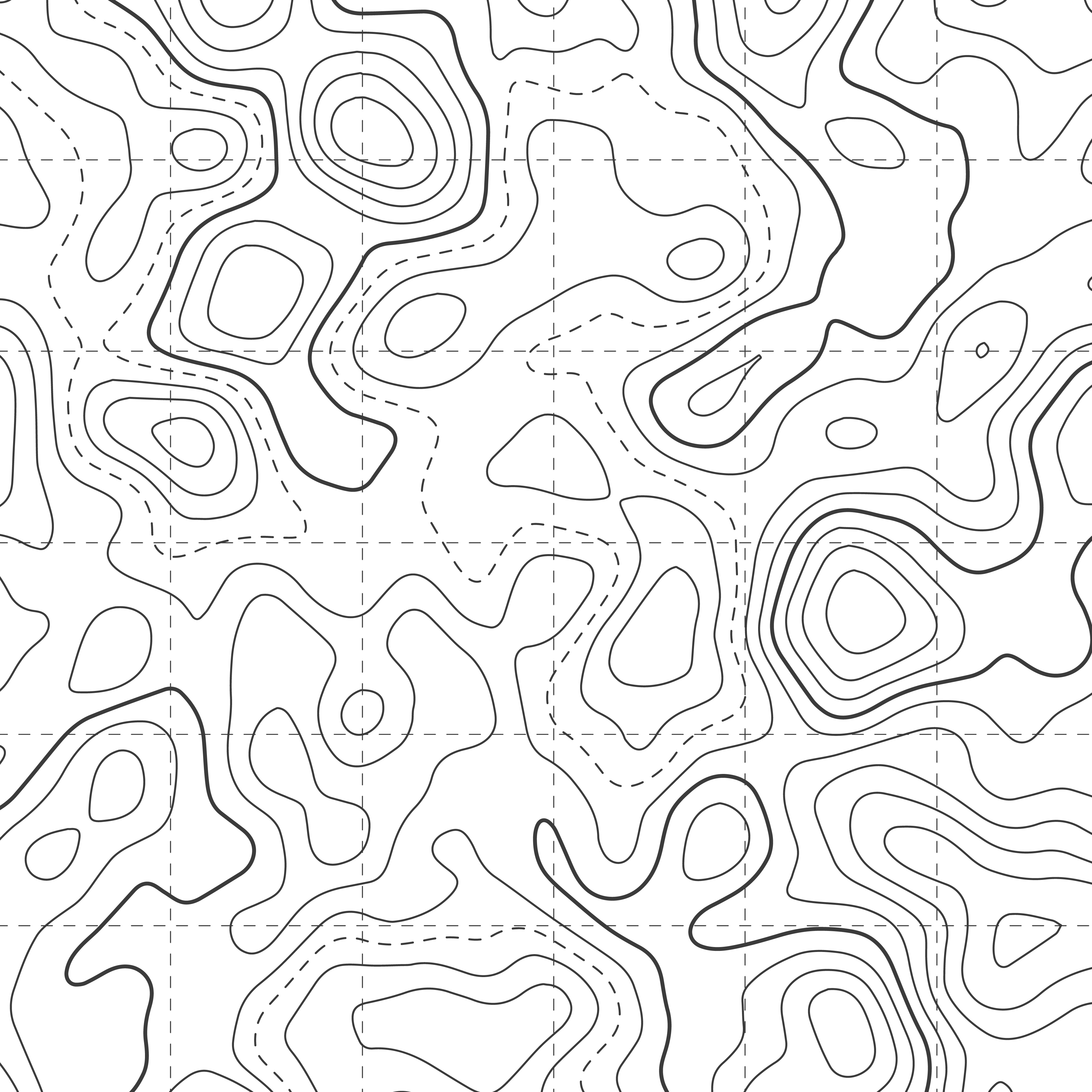
topographic map diagram pattern background Download Free Vector Art
It is also important to note that land patterns should always match with the arrangements of lead. So, why is it essential? News and world.

Artist Arranges Rocks And Leaves Into Beautiful Geometric Land Art
Ball size on the component. So, why is it essential? Lga + pin qty + c + pitch p + pin columns x pin rows.

Project 17 Agricultural Aerial Land Patterns 1 on Behance
Land pads are always a little larger than part pads. Here, the land pattern needs to be designed to accommodate the solder fillet on each.

Project 17 Agricultural Aerial Land Patterns 1 on Behance
The land pattern on a circuit board matches the arrangement of leads on a component. The heterogeneity of these patterns is the main focus of.

Project 17 Agricultural Aerial Land Patterns 1 on Behance
Web a land pattern is the arrangement of pads on a circuit board. Land patterns specify where copper will exist on fabrication layers. Lga +.
LAND PATTERN
Web the land pattern refers to the size of the pads and outline for a given part that should be designed onto a pcb. Web.

Project 17 Agricultural Aerial Land Patterns 1 on Behance
The land pattern is usually built using ecad library tools. Lga + pin qty + c + pitch p + pin columns x pin rows.
Project 17 Agricultural Aerial Land Patterns 1 on Behance
Surface mount land patterns, also referred to as footprints or pads, define the sites at which components are to be soldered to a printed circuit.
Significant Effort Needs To Be Made To Ensure They Are Accurate.
This document provides generic requirements on land pattern geometries used for the surface attachment of electronic components, as well as surface mount design recommendations for achieving the best possible solder joints to the devices assembled. By the end of this video you will know what to include in your land pattern regardless of your pcb design software tool. Web a land pattern is the arrangement of pads on a circuit board. The heterogeneity of these patterns is the main focus of landscape ecology.
Web Generic Requirements For Surface Mount Design And Land Pattern Standard.
Web the results show that socioeconomic development can lead to rapid changes in land use patterns, especially in cultivated and construction land. Web the land pattern refers to the size of the pads and outline for a given part that should be designed onto a pcb. Not surprisingly, economic geographers use economic reasons to explain the location of economic activities. It is also important to note that land patterns should always match with the arrangements of lead.
From Baby To Adult, We Have Patterns For Every Size And Skill Level.
Primarily, a land pattern attaches and connects the electronic component on a circuit board depending on the layout and the design of the board. Primarily, a land pattern attaches and connects the electronic component on a circuit board depending on the layout and the design of the board. This book chapter emphasizes the significance of categorical raster data in ecological studies, specifically land use or land cover (lulc) data, and highlights the pivotal role of landscape metrics and. Web first set of equations and land pattern dimensions.
Surface Mount Land Patterns, Also Referred To As Footprints Or Pads, Define The Sites At Which Components Are To Be Soldered To A Printed Circuit Board.
The collection of copper traces, soldermask openings, silkscreen, and other features that define the part on the pcb. Lga + pin qty + s + pitch p + pin columns x pin rows _ body length x body width x height. Here, the land pattern needs to be designed to accommodate the solder fillet on each edge of the lead, which is quantified with the three j values. Land patterns specify where copper will exist on fabrication layers.