Kikuchi Pattern - Web kikuchi pattern are in a range from 13 kev at the bottom of the pattern to below 11 kev. The model considers the result of two combined mechanisms: Google scholar thomas, g (1978) in modern diffraction and imaging technique in materials science p 399 eds. Rules for generating and using stereographic projections for solving problems in crystallography are presented. The mask can take whatever shape we want, as long as it is a boolean array of the detector. Kikuchi lines are patterns of electrons formed by scattering. Web the kikuchi pattern simulation is based on the kinematic theory of diffraction, with kikuchi line intensities computed via a discrete structure factor calculation. This method is validated using single crystal atomistic models, and. Web a grid of kikuchi patterns is collected by scanning the electron beam across the sample surface. The camera length for the following experiments was therefore.
1 Stereographic projection of the dynamically simulated Kikuchi
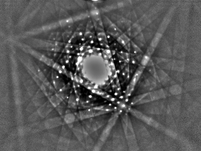
Web kikuchi lines often appear on electron diffraction patterns: A pair of kikuchi lines is arrowed. Y = − x a − x b y.

Typical Kikuchi patterns for the austenitemartensite transition under
From one kikuchi pattern we can extend the lines to cre ate a second pattern. Web for the case of electron diffraction, these patterns from.
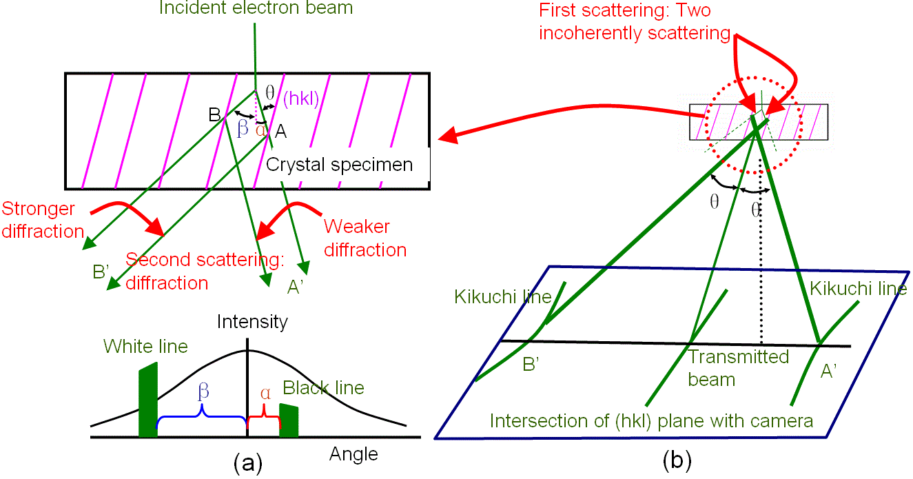
Kikuchi lines & bands in electron diffraction
Google scholar thomas, g (1978) in modern diffraction and imaging technique in materials science p 399 eds. Web map of kikuchi line pairs down to.
Transmission Kikuchi Diffraction Oxford NanoAnalysis
Notice that we can define all the distances in terms of their equivalent angles, as in any dp. These patterns are then indexed to form.

Kikuchi patterns showing the orientation difference across bent fine
A pair of kikuchi lines is arrowed. Web map of kikuchi line pairs down to 1/1å for 300 kev electrons in hexagonal sapphire (al 2.

Kikuchi patterns observed in yellow glass beads (a) and assigned to
A pair of kikuchi lines is arrowed. A pair of kikuchi lines is arrowed. Web a grid of kikuchi patterns is collected by scanning the.
2.11. Kikuchi Lines — Introduction to Transmisison Electron Microscopy
Web kikuchi pattern are in a range from 13 kev at the bottom of the pattern to below 11 kev. Y = − x a.

Kikuchi patterns of (a) orthorhombic YBCO, (b) tetragonal YBCO and (c
Positions on the phosphor screen show an increase in their spread, as we characterize here. A pair of kikuchi lines is arrowed. Furthermore, the bse.
Schematic diagram of a pair of Kikuchi lines, that is Kikuchi band
From one kikuchi pattern we can extend the lines to cre ate a second pattern. Web we discuss a refined simulation approach which treats kikuchi.

Kikuchi patterns from Electron Backscatter Diffraction of selected
Kikuchi lines are patterns of electrons formed by scattering. Inelastically scattered electrons play an important role in the formation of the rheed pattern. For example,.
For Pattern Indexing, The Latter Intensity Is Undesirable, While For Virtual Backscatter Electron Vbse) Imaging, This Intensity Can Reveal Topographical, Compositional Or Diffraction Contrast.
The kikuchi lines are the bisections of lines from the center spot to the bragg spots. The camera length for the following experiments was therefore. In such cases, we can pass a signal mask to exclude the pixels where the mask values are true. Beyond the mere extraction of the crystallographic orientation from the kikuchi pattern, it.
Positions On The Phosphor Screen Show An Increase In Their Spread, As We Characterize Here.
A pair of kikuchi lines is arrowed. This method is validated using single crystal atomistic models, and. An increased solid angle will improve reliability and confidence in pattern indexing, as well as reduce the 180° orientation ambiguity [13]. Notice that we can define all the distances in terms of their equivalent angles, as in any dp.
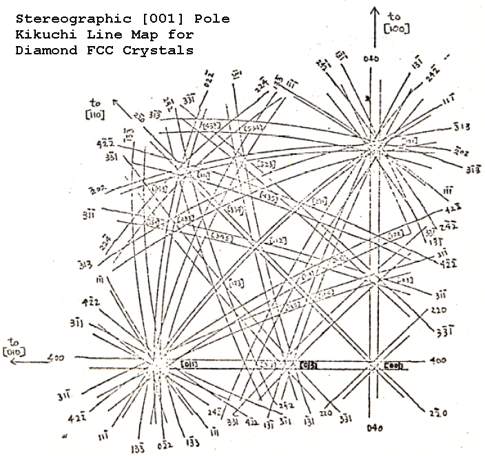
Web Map Of Kikuchi Line Pairs Down To 1/1Å For 300 Kev Electrons In Hexagonal Sapphire (Al 2 O 3), With Some Intersections Labeled.
So we draw the 020 and 020 lines from the [001] pole 45° to the [101] pole. Google scholar thomas, g (1978) in modern diffraction and imaging technique in materials science p 399 eds. Kikuchi lines often appear on electron diffraction patterns: For example, knowing the [001] pattern we can con struct the [101] pattern since a pair of lines is common to both.
Web Ebsp Pattern Processing Serves The Purpose To Process The Measured Raw Pattern Data In Such A Way That The Crystallographic Information Stored In The Kikuchi Diffraction Pattern Can Be Extracted In The Fastest Way By The Subsequent “Indexing” Steps.
Web for the case of electron diffraction, these patterns from incoherent internal sources are called kikuchi patterns. Y = − x a − x b y a − y b x + x a 2 − x b 2 + y a 2 − y b 2 2 ⋅ ( y a − y b) Web kikuchi patterns in the sem: To illustrate the connections between various electron diffraction methods, the formation of kikuchi bands in electron backscatter diffraction in the.