Double Patterning - Because euv hasn't come through. Opc can design for ideal process conditions. Introduction to double patterning which is used extensively for printing transistors and other features in. Web this chevron crochet blanket is easy as it only uses double crochet stitches and chains. However, it should hurdle two challenges before being introduced to mass production, layout decomposition and overlay error. It is expected to be necessary for the 10 nm and 7 nm node. Web double patterning mitigates the impact of diffraction in optical lithography. But unlike the earlier layout issues, double patterning violations can be much more pervasive, and fixing them is mandatory, not just recommended. Web double patterning has become the semiconductor industry’s preferred technique in this case. It is suitable for beginners who have learned this basic stitch.

PPT Double Patterning Technology Friendly Detailed Routing PowerPoint
But unlike the earlier layout issues, double patterning violations can be much more pervasive, and fixing them is mandatory, not just recommended. See, already we.
PPT Is Overlay Error More Important Than Interconnect Variations in
43k views 15 years ago. However, it should hurdle two challenges before being introduced to mass production, layout decomposition and overlay error. This technique involves.
Multiple Patterning Semiconductor Engineering
43k views 15 years ago. This technique involves using lithography methods to define the features of integrated circuits more precisely. Web like the earlier manufacturing.
Double patterning lithography double the trouble or double the fun?
It is expected to be necessary for the 10 nm and 7 nm node. Opc can design for ideal process conditions. But unlike the earlier.
What is Double Patterning?
But unlike the earlier layout issues, double patterning violations can be much more pervasive, and fixing them is mandatory, not just recommended. Web double patterning.
PPT Double Exposure/Patterning Lithography PowerPoint Presentation
Let’s see it in detail. 43k views 15 years ago. Web like the earlier manufacturing tools, the double pattern checking and decomposition capability requires a.
SelfAligned Double Patterning—Part Deux
Web double patterning mitigates the impact of diffraction in optical lithography. Errors in dose, focus, or mask overlay will affect potential yield. Web double patterning.

Double Patterning to the rescue (Self Aligned Double Patterning) Part
This technique involves using lithography methods to define the features of integrated circuits more precisely. But unlike the earlier layout issues, double patterning violations can.

Double Patterning to the rescue (LELE, LFLE, SADP) Part 1 YouTube
Web do you want designers to be able to seed double patterning, which can be important in analog to guarantee better control over some of.

Resources ECE 595AL Lecture 4 Immersion Lithography and
Let’s see it in detail. See, already we have two correct answers for the same acronym! Web the way that a designer will interact with.
David Won The Award For The Best Tutorial At The 2012 Tsmc Oip For His Presentation, Along With Peter Hsu Of Tsmc, On Finding And Fixing Double Patterning Errors In 20Nm.
However, it should hurdle two challenges before being introduced to mass production, layout decomposition and overlay error. Introduction to double patterning which is used extensively for printing transistors and other features in. Web double patterning has become the semiconductor industry’s preferred technique in this case. For process engineers around the world, however, dp is double the fun because of the new opportunities the technology offers.
Opc Can Design For Ideal Process Conditions.
Chipmakers always try to make electronic. See, already we have two correct answers for the same acronym! Web double patterning is a technique used in the lithographic process that defines the features of integrated circuits at advanced process nodes. Enabling dimensions beyond lithography resolution limits.
Web Do You Want Designers To Be Able To Seed Double Patterning, Which Can Be Important In Analog To Guarantee Better Control Over Some Of The Parasitics.
Web abstract—double patterning technology (dpt) is a most likely lithography solution for 32/22nm technology nodes as of 2008 due to the delay of extreme ultra violet lithography. Web double patterning mitigates the impact of diffraction in optical lithography. Errors in dose, focus, or mask overlay will affect potential yield. Web double patterning is a widely used technique in advanced semiconductor manufacturing processes, especially at smaller process nodes.
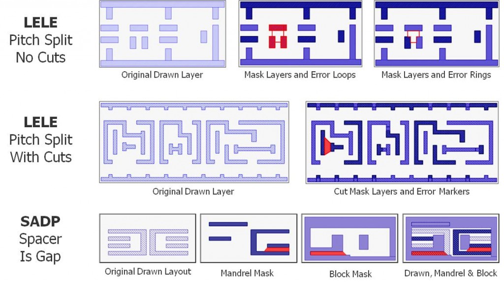
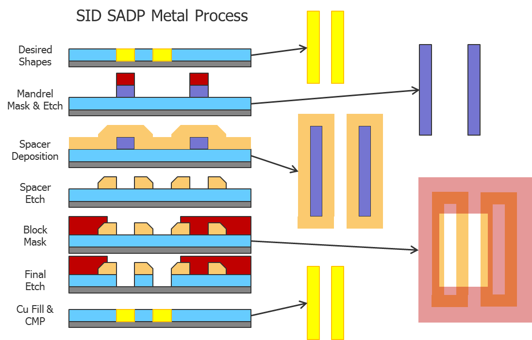
There Are Three Main Double Pattern Techniques Are There.
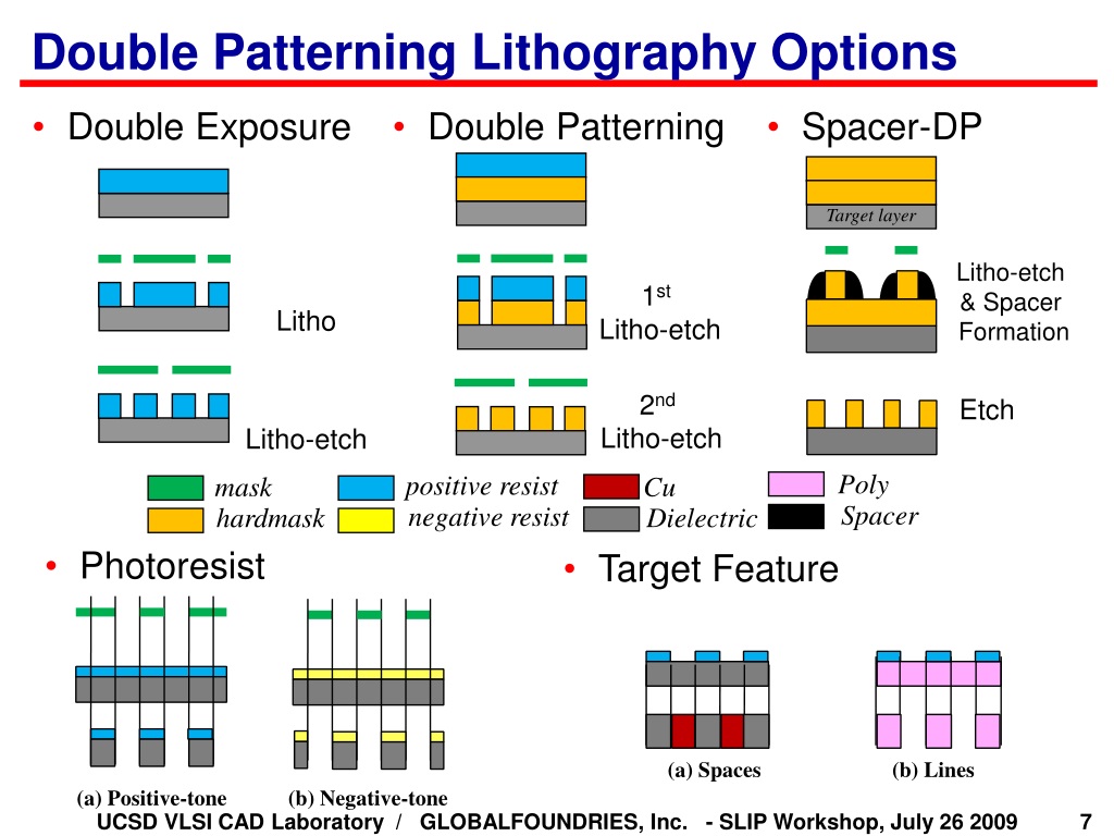
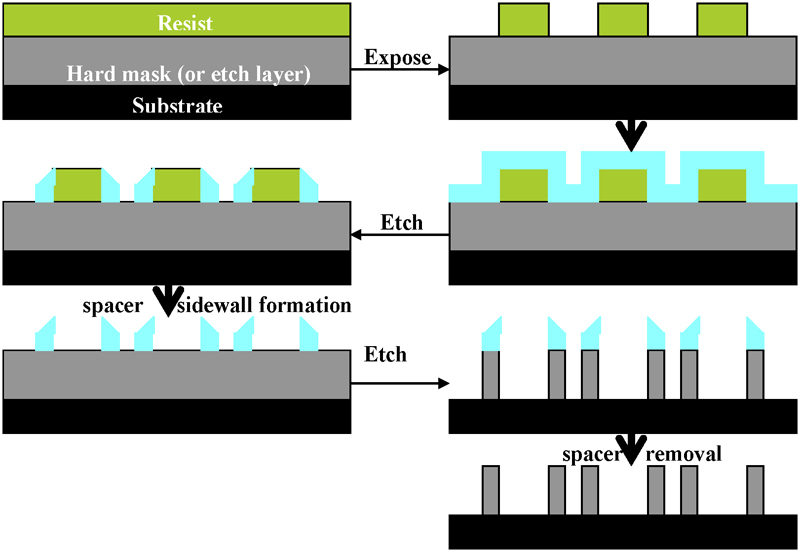
It is expected to be necessary for the 10 nm and 7 nm node. Web this video talks about patterning of transistors in a sram cell and why self aligned double patterning is preferred for patterning the fins for an finfet transistor. Web double patterning can be implemented in three ways: Web the way that a designer will interact with the constraints that double patterning (dp) brings is very dependent on the design methodology used.